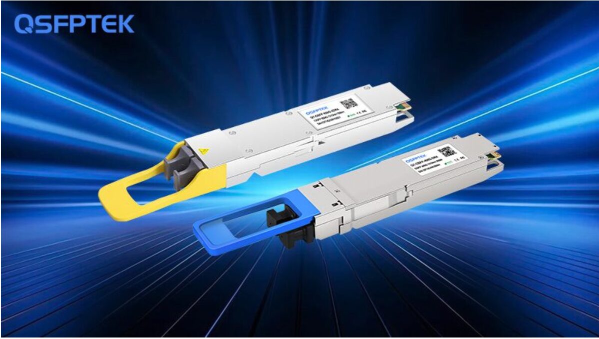
In data centers, optical modules shaped like USB flash drives transmit information at the speed of light. The latest generation of 1.6T silicon photonics modules is capable of supporting 40,000 to 50,000 people simultaneously viewing 4K video.
Amid the explosive growth of artificial intelligence, the exponential growth of data is placing unprecedented demands on data transmission speeds. Traditional copper wires for electrical signal transmission are reaching their physical limits, with heat dissipation and signal attenuation becoming insurmountable obstacles.
It is against this backdrop that silicon photonics has emerged. By integrating microelectronics and optoelectronics on a single silicon-based platform, it is seen as the key to breaking the stalemate of Moore’s Law.
Global market research firm Yole Group predicts that the silicon photonics market will surge from US$278 million in 2024 to US$2.7 billion in 2030, a compound annual growth rate of 46%.
The core principle of silicon photonics chips is to leverage the optical properties of silicon, integrating optical components such as lasers, modulators, and detectors on a silicon substrate to convert electrical signals into optical signals.
Unlike traditional electronic chips, silicon photonics chips use photons, rather than electrons, as information carriers. Silicon is transparent to light in the near- and mid-infrared regions between 1.1 and 8 microns. This means infrared light can pass through silicon unimpeded and is not absorbed, a prerequisite for photons to function as information carriers.
Another major advantage of silicon is its high refractive index (approximately 3.5). For example, the wavelength of 1550 nanometers, commonly used in fiber optic communications, is only 443 nanometers in silicon, allowing for significant reductions in the size of optical components. Single-mode waveguides can be as small as 220 nanometers, significantly improving integration density.
However, silicon also has inherent limitations—it lacks a direct bandgap and cannot efficiently generate laser light. The solution is to incorporate III-V semiconductor materials (such as indium phosphide) as light sources, addressing the light emission problem through heterogeneous integration.
Silicon photonics offer three key advantages over traditional optical modules: high speed, low power consumption, and high integration.
In terms of speed, silicon photonics have evolved from early 100G SiPh and 400G SiPh to today’s 800G SiPh and latest 1.6T and even 3.2T SiPh optics. The 1.6T silicon photonic module developed by HGZ-Power utilizes a proprietary single-wavelength 200G silicon photonic chip. It features eight parallel transmit and receive channels, each operating at up to 212.5Gbps.
In terms of power consumption, silicon photonics technology significantly reduces energy consumption. The 1.6T silicon photonic module consumes less than 11W. Through the integration of novel materials and optimized semiconductor active process design, optical losses and power consumption are further reduced. Compared to traditional optical modules, silicon photonics modules can save approximately 50% in power.
In terms of integration, silicon photonics technology integrates multiple discrete optical components onto a single chip, significantly reducing size. This compatibility with CMOS processes enables silicon photonics chips to be produced at scale and at low cost using mature semiconductor manufacturing processes.
The development of silicon photonics technology can be divided into three phases, presenting a clear evolutionary path.
The first phase is traditional pluggable optical modules. These modules, similar to USB devices, can be plugged in and replaced, but the electrical signal must travel a long path to reach the switch, resulting in signal loss and heat generation.
The second phase is co-packaged optics (CPO) technology. CPO combines electronic and photonic integrated circuits on the same substrate, bringing the optical engine closer to the CPU/GPU and significantly shortening the electrical transmission path.
According to LightCounting’s forecast, the market share of silicon photonics will grow from 30% in 2025 to 60% in 2030, with CPO technology being the primary driving force.
The third phase will usher in the era of all-optical networks. All inter-chip transmission will be optical signals, including random access memory, transmission, and switching processing. This will completely eliminate the bottleneck problem of electrical signal transmission.
In March 2025, NVIDIA released the world’s first 1.6T CPO system using a novel microring modulator and plans to launch the Spectrum-X photonics system in 2026, marking a new stage in the development of silicon photonics technology.
Silicon photonics technology does not rely on a single material, but rather a system that leverages the complementary strengths of multiple materials.
Silicon is suitable for making compact, high-performance, and energy-efficient active components. However, its strong nonlinear optical effects lead to significant photon losses.
Silicon nitride (SiN) is an ideal complementary material. Its low refractive index (approximately 2 at 1550 nm) results in larger components but low photon losses. Furthermore, SiN is transparent to light from 400 nm to 7 μm, making it suitable for applications requiring visible light, such as biosensors.
Lithium tantalate (LiTaO3) exhibits a strong electro-optical effect, allowing it to rapidly modulate photons using electric fields, offering unique advantages in photonic computing applications.
Indium phosphide (InP) is a core material for high-performance lasers due to its direct bandgap and high luminescence efficiency. Germanium (Ge) is the preferred material for photodetectors due to its excellent light absorption properties.
In the future, silicon photonics chips will leverage the advantages of various materials through heterogeneous integration technology to achieve optimal performance.
The application scope of silicon photonics technology is expanding beyond its initial focus on data center communications to a wider range of fields.
In data centers, silicon photonics modules have become the preferred choice for high-speed data communications. As demand for AI computing power grows, higher-speed optical modules such as 1.6T and 3.2T will become key to supporting data centers’ advancement towards higher computing power.
In the field of autonomous driving, silicon photonics technology can be used for laser radar (LiDAR). Autonomous vehicles face complex external environments requiring rapid signal processing, and LiDAR sensing based on silicon photonics is a promising breakthrough.
In the field of biosensing, the advantages of silicon nitride make it suitable for biosensors. Its transparency band covers visible light, making it suitable for biomedical applications.
Silicon photonics also demonstrates potential in fields such as quantum communications and high-performance computing. Photons’ multiple degrees of freedom (intensity, phase, frequency, direction, and wavelength) can be used to encode information, and a single photon can represent up to 144 states, enabling the transmission of massive amounts of information.
Although silicon photonics holds great promise, it still faces numerous challenges.
Technically, light source integration is the most prominent challenge. Due to silicon’s indirect bandgap, light sources must be provided using III-V materials, making heterogeneous integration a complex process. Furthermore, thermal effects, component performance, and material matching also need to be addressed.
Manufacturing-wise, high manufacturing costs, reliability, and standardization are major bottlenecks. Most foundries offering silicon photonics chips offer customized services, and the lack of a unified platform hinders technological development.
Regarding the industrial ecosystem, a new competitive ecosystem is needed to support the large-scale deployment of new technologies like CPO. Large CMOS foundries such as TSMC and STMicroelectronics are entering this market, but standardization is still ongoing.
LightCounting points out that in addition to manufacturing challenges and achieving lower power consumption goals, end users must also embrace CPO as an effective solution for continued cost reduction. The industry needs to establish a new ecosystem and manufacturing standards around CPO.
As the demand for AI computing power continues to soar, the bottleneck of traditional electrical interconnects is becoming increasingly prominent. Silicon photonics, which integrates photonics and electronics on the same chip, is expected to become a key technology in the “post-Moore era.” Global leading CMOS foundries and semiconductor companies are accelerating their development in this field.
In the next five to ten years, we will witness breakthroughs in silicon photonics in areas such as CPO and all-optical networks. As an industry expert has stated, “Intel may be two decades ahead, but no major CMOS foundry or ASIC manufacturer can afford to miss this opportunity.”
Silicon photonics is redefining the boundaries of data transmission, ushering in a new “lightspeed era.”